128Mb, 256Mb, 512Mb, 1Gb StrataFlash Memory
Features
Micron StrataFlash Embedded Memory
P/N
P/N
P/N
P/N
–
–
–
–
PC28F128G18xx
PC28F256G18xx
PC28F512G18xx
PC28F00AG18xx
Features
• Power
– Core voltage: 1.7 V - 2.0 V
– I/O voltage: 1.7 V - 2.0 V
– Standby current: 60 μA (typ) for 512-Mbit, 65 nm
– Deep Power-Down mode: 2 μA (typ)
– Automatic Power Savings mode
– 16-word synchronous-burst read current: 23 mA
(typ) @ 108 MHz; 24 mA (typ) @ 133 MHz
• Software
– Micron® Flash data integrator (FDI) optimized
– Basic command set (BCS) and extended command set (ECS) compatible
– Common Flash interface (CFI) capable
• Security
– One-time programmable (OTP) space
64 unique factory device identifier bits
2112 user-programmable OTP bits
– Absolute write protection: V PP = GND
– Power-transition erase/program lockout
– Individual zero latency block locking
– Individual block lock-down
• Density and packaging
– 128Mb, 256Mb, 512Mbit, and 1-Gbit
– Address-data multiplexed and non-multiplexed
interfaces
– 64-Ball Easy BGA
• High-Performance Read, Program and Erase
– 96 ns initial read access
– 108 MHz with zero wait-state synchronous burst
reads: 7 ns clock-to-data output
– 133 MHz with zero wait-state synchronous burst
reads: 5.5 ns clock-to-data output
– 8-, 16-, and continuous-word synchronous-burst
Reads
– Programmable WAIT configuration
– Customer-configurable output driver impedance
– Buffered Programming: 2.0 μs/Word (typ), 512Mbit 65 nm
– Block Erase: 0.9 s per block (typ)
– 20 μs (typ) program/erase suspend
• Architecture
– 16-bit wide data bus
– Multi-Level Cell Technology
– Symmetrically-Blocked Array Architecture
– 256-Kbyte Erase Blocks
– 1-Gbit device: Eight 128-Mbit partitions
– 512-Mbit device: Eight 64-Mbit partitions
– 256-Mbit device: Eight 32-Mbit partitions
– 128-Mbit device: Eight 16-Mbit partitions
– Read-While-Program and Read-While-Erase
– Status Register for partition/device status
– Blank Check feature
• Quality and Reliability
– Expanded temperature: –30 °C to +85 °C
– Minimum 100,000 erase cycles per block
– 65nm Process Technology
PDF: 09005aef8448483a
128_256_512_65nm_g18.pdf - Rev. E 8/11 EN
1
Micron Technology, Inc. reserves the right to change products or specifications without notice.
© 2011 Micron Technology, Inc. All rights reserved.
Products and specifications discussed herein are subject to change by Micron without notice.
�128Mb, 256Mb, 512Mb, 1Gb StrataFlash Memory
Features
Contents
General Description ......................................................................................................................................... 8
Functional Overview ........................................................................................................................................ 8
Configuration and Memory Map ....................................................................................................................... 9
Device ID ....................................................................................................................................................... 12
Package Dimensions ....................................................................................................................................... 13
Signal Assignments ......................................................................................................................................... 14
Signal Descriptions ......................................................................................................................................... 15
Bus Interface .................................................................................................................................................. 16
Reset .......................................................................................................................................................... 16
Standby ..................................................................................................................................................... 16
Output Disable ........................................................................................................................................... 16
Asynchronous Read .................................................................................................................................... 17
Synchronous Read ...................................................................................................................................... 17
Burst Wrapping .......................................................................................................................................... 17
End-of-Wordline Delay ............................................................................................................................... 18
Write .......................................................................................................................................................... 19
Command Definitions .................................................................................................................................... 20
Status Register ................................................................................................................................................ 23
Clear Status Register ................................................................................................................................... 24
Read Configuration Register ........................................................................................................................... 25
Programming the Read Configuration Register ............................................................................................ 26
Extended Configuration Register ..................................................................................................................... 27
Output Driver Control ................................................................................................................................ 27
Programming the Extended Configuration Register ...................................................................................... 28
Read Operations ............................................................................................................................................. 29
Read Array ................................................................................................................................................. 29
Read ID ...................................................................................................................................................... 29
Read CFI .................................................................................................................................................... 30
Read Status Register ................................................................................................................................... 30
WAIT Operation ......................................................................................................................................... 31
Programming Modes ...................................................................................................................................... 32
Control Mode ............................................................................................................................................. 32
Object Mode .............................................................................................................................................. 33
Program Operations ....................................................................................................................................... 37
Single-Word Programming .......................................................................................................................... 37
Buffered Programming ............................................................................................................................... 38
Buffered Enhanced Factory Programming ................................................................................................... 38
Erase Operations ............................................................................................................................................ 41
BLOCK ERASE ............................................................................................................................................ 41
SUSPEND and RESUME Operations ................................................................................................................ 42
SUSPEND Operation .................................................................................................................................. 42
RESUME Operation .................................................................................................................................... 43
BLANK CHECK Operation .............................................................................................................................. 44
Block Lock ..................................................................................................................................................... 45
One-Time Programmable Operations .............................................................................................................. 47
Programming OTP Area .............................................................................................................................. 49
Reading OTP Area ....................................................................................................................................... 49
Global Main-Array Protection ......................................................................................................................... 50
Dual Operation .............................................................................................................................................. 51
Power and Reset Specifications ....................................................................................................................... 52
PDF: 09005aef8448483a
128_256_512_65nm_g18.pdf - Rev. E 8/11 EN
2
Micron Technology, Inc. reserves the right to change products or specifications without notice.
© 2011 Micron Technology, Inc. All rights reserved.
�128Mb, 256Mb, 512Mb, 1Gb StrataFlash Memory
Features
Initialization .............................................................................................................................................. 52
Power-Up and Down .................................................................................................................................. 52
Reset .......................................................................................................................................................... 52
Automatic Power Saving ............................................................................................................................. 54
Power Supply Decoupling ........................................................................................................................... 54
Electrical Specifications .................................................................................................................................. 55
Electrical Specifications – DC Current and Voltage Characteristics and Operating Conditions ............................ 56
Electrical Specifications – AC Characteristics and Operating Conditions ........................................................... 60
AC Test Conditions ..................................................................................................................................... 60
AC Read Specifications ................................................................................................................................... 62
AC Read Specifications (CLK-Latching, 133 MHz) ........................................................................................ 62
AC Read Timing .......................................................................................................................................... 63
AC Write Specifications ................................................................................................................................... 72
Electrical Specifications – Program/Erase Characteristics ................................................................................. 79
Common Flash Interface ................................................................................................................................ 80
READ CFI Structure Output ........................................................................................................................ 80
CFI ID String .............................................................................................................................................. 81
System Interface Information ...................................................................................................................... 81
Device Geometry Definition ....................................................................................................................... 82
Primary Micron-Specific Extended Query .................................................................................................... 85
Flowcharts ..................................................................................................................................................... 91
AADM Mode ................................................................................................................................................. 108
AADM Feature Overview ............................................................................................................................ 108
AADM Mode Enable (RCR[4] = 1) ............................................................................................................... 108
Bus Cycles and Address Capture ................................................................................................................. 108
WAIT Behavior .......................................................................................................................................... 108
Asynchronous READ and WRITE Cycles ..................................................................................................... 109
Asynchronous READ Cycles ....................................................................................................................... 109
Asynchronous WRITE Cycles ..................................................................................................................... 111
Synchronous READ and WRITE Cycles ....................................................................................................... 112
Synchronous READ Cycles ......................................................................................................................... 112
Synchronous WRITE Cycles ....................................................................................................................... 115
System Boot .............................................................................................................................................. 115
Ordering Information .................................................................................................................................... 116
Revision History ............................................................................................................................................ 117
Rev. E – 8/11 .............................................................................................................................................. 117
Rev. D – 5/11 ............................................................................................................................................. 117
Rev. C – 2/11 .............................................................................................................................................. 117
Rev. B – 12/10 ............................................................................................................................................ 117
Rev. A – 12/10 ............................................................................................................................................ 117
PDF: 09005aef8448483a
128_256_512_65nm_g18.pdf - Rev. E 8/11 EN
3
Micron Technology, Inc. reserves the right to change products or specifications without notice.
© 2011 Micron Technology, Inc. All rights reserved.
�128Mb, 256Mb, 512Mb, 1Gb StrataFlash Memory
Features
List of Figures
Figure 1: 64-Ball Easy BGA (8mm x 10mm x 1.2mm) ....................................................................................... 13
Figure 2: 64-Ball Easy BGA (Top View, Balls Down) ......................................................................................... 14
Figure 3: Main Array Word Lines .................................................................................................................... 18
Figure 4: Wrap/No-Wrap Example ................................................................................................................. 18
Figure 5: End-of-Wordline Delay .................................................................................................................... 18
Figure 6: Two-Cycle Command Sequence ....................................................................................................... 20
Figure 7: Single-Cycle Command Sequence .................................................................................................... 20
Figure 8: READ Cycle Between WRITE Cycles ................................................................................................. 20
Figure 9: Illegal Command Sequence ............................................................................................................. 21
Figure 10: Configurable Programming Regions: Control Mode and Object Mode .............................................. 33
Figure 11: Configurable Programming Regions: Control Mode and Object Mode Segments .............................. 35
Figure 12: BLOCK LOCK Operations ............................................................................................................... 46
Figure 13: OTP Area Map ............................................................................................................................... 48
Figure 14: V PP Supply Connection Example .................................................................................................... 50
Figure 15: RESET Operation Waveforms ......................................................................................................... 53
Figure 16: AC Input/Output Reference Waveform ........................................................................................... 60
Figure 17: Transient Equivalent Testing Load Circuit ....................................................................................... 60
Figure 18: Clock Input AC Waveform .............................................................................................................. 61
Figure 19: Asynchronous Page-Mode Read (Non-MUX) .................................................................................. 64
Figure 20: Synchronous 8- or 16-Word Burst Read (Non-MUX) ........................................................................ 65
Figure 21: Synchronous Continuous Misaligned Burst Read (Non-MUX) ......................................................... 66
Figure 22: Synchronous Burst with Burst Interrupt Read (Non-MUX) .............................................................. 67
Figure 23: Asynchronous Single-Word Read .................................................................................................... 68
Figure 24: Synchronous 8- or 16-Word Burst Read (A/D MUX) ......................................................................... 69
Figure 25: Synchronous Continuous Misaligned Burst Read (A/D MUX) .......................................................... 70
Figure 26: Synchronous Burst with Burst-Interrupt (AD-Mux) ......................................................................... 70
Figure 27: Write Timing ................................................................................................................................. 73
Figure 28: Write to Write (Non-Mux) .............................................................................................................. 74
Figure 29: Async Read to Write (Non-Mux) ..................................................................................................... 74
Figure 30: Write to Async Read (Non-Mux) ..................................................................................................... 75
Figure 31: Sync Read to Write (Non-Mux) ....................................................................................................... 75
Figure 32: Write to Sync Read (Non-Mux) ....................................................................................................... 76
Figure 33: Write to Write (AD-Mux) ................................................................................................................ 76
Figure 34: Async Read to Write (AD-Mux) ....................................................................................................... 77
Figure 35: Write to Async Read (AD-Mux) ....................................................................................................... 77
Figure 36: Sync Read to Write (AD-Mux) ......................................................................................................... 78
Figure 37: Write to Sync Read (AD-Mux) ......................................................................................................... 78
Figure 38: Word Program Procedure ............................................................................................................... 91
Figure 39: Word Program Full Status Check Procedure .................................................................................... 92
Figure 40: Program Suspend/Resume Procedure ............................................................................................ 93
Figure 41: Buffer Programming Procedure ...................................................................................................... 95
Figure 42: Buffered Enhanced Factory Programming (BEFP) Procedure ........................................................... 97
Figure 43: Block Erase Procedure ................................................................................................................... 99
Figure 44: Block Erase Full Status Check Procedure ........................................................................................ 100
Figure 45: Erase Suspend/Resume Procedure ................................................................................................ 101
Figure 46: Block Lock Operations Procedure .................................................................................................. 103
Figure 47: Protection Register Programming Procedure ................................................................................. 104
Figure 48: Protection Register Programming Full Status Check Procedure ....................................................... 105
Figure 49: Blank Check Procedure ................................................................................................................. 106
Figure 50: Blank Check Full Status Check Procedure ...................................................................................... 107
PDF: 09005aef8448483a
128_256_512_65nm_g18.pdf - Rev. E 8/11 EN
4
Micron Technology, Inc. reserves the right to change products or specifications without notice.
© 2011 Micron Technology, Inc. All rights reserved.
�128Mb, 256Mb, 512Mb, 1Gb StrataFlash Memory
Features
Figure 51:
Figure 52:
Figure 53:
Figure 54:
Figure 55:
Figure 56:
Figure 57:
Figure 58:
AADM Asynchronous READ Cycle (Latching A[MAX:0]) ................................................................. 110
AADM Asynchronous READ Cycle (Latching A[15:0] only) .............................................................. 110
AADM Asynchronous WRITE Cycle (Latching A[MAX:0]) ................................................................ 111
AADM Asynchronous WRITE Cycle (Latching A[15:0] only) ............................................................ 112
AADM Synchronous Burst READ Cycle (ADV# De-asserted Between Address Cycles) ....................... 113
AADM Synchronous Burst READ Cycle (ADV# Not De-asserted Between Address Cycles) ................ 114
AADM Synchronous Burst READ Cycle (Latching A[15:0] only) ....................................................... 114
Part Number Chart for G18 Components ....................................................................................... 116
PDF: 09005aef8448483a
128_256_512_65nm_g18.pdf - Rev. E 8/11 EN
5
Micron Technology, Inc. reserves the right to change products or specifications without notice.
© 2011 Micron Technology, Inc. All rights reserved.
�128Mb, 256Mb, 512Mb, 1Gb StrataFlash Memory
Features
List of Tables
Table 1: Main Array Memory Map – 128Mb, 256Mb ........................................................................................... 9
Table 2: Main Array Memory Map – 512Mb, 1Gb ............................................................................................. 10
Table 3: Device ID Codes ............................................................................................................................... 12
Table 4: Signal Descriptions ........................................................................................................................... 15
Table 5: Bus Control Signals ........................................................................................................................... 16
Table 6: Command Set .................................................................................................................................. 21
Table 7: Status Register Bit Definitions (Default Value = 0080h) ....................................................................... 23
Table 8: CLEAR STATUS REGISTER Command Bus Cycles ............................................................................... 24
Table 9: Read Configuration Register Bit Definitions (Default Value = BFCFh) .................................................. 25
Table 10: Supported Clock Frequencies .......................................................................................................... 25
Table 11: PROGRAM READ CONFIGURATION REGISTER Bus Cycles .............................................................. 26
Table 12: Extended Configuration Register Bit Definitions (Default Value = 0004h) ........................................... 27
Table 13: Output Driver Control Characteristics .............................................................................................. 27
Table 14: Program Extended Configuration Register Command Bus Cycles ...................................................... 28
Table 15: READ MODE Command Bus Cycles ................................................................................................. 29
Table 16: Device Information ......................................................................................................................... 30
Table 17: WAIT Behavior Summary – Non-MUX ............................................................................................. 31
Table 18: WAIT Behavior Summary – AD MUX ................................................................................................ 31
Table 19: Programming Region Next State ...................................................................................................... 36
Table 20: PROGRAM Command Bus Cycles .................................................................................................... 37
Table 21: BEFP Requirements and Considerations .......................................................................................... 39
Table 22: ERASE Command Bus Cycle ............................................................................................................ 41
Table 23: Valid Commands During Suspend ................................................................................................... 42
Table 24: SUSPEND and RESUME Command Bus Cycles ................................................................................ 43
Table 25: BLANK CHECK Command Bus Cycles ............................................................................................. 44
Table 26: BLOCK LOCK Command Bus Cycles ................................................................................................ 45
Table 27: Block Lock Configuration ................................................................................................................ 46
Table 28: Program OTP Area Command Bus Cycles ......................................................................................... 47
Table 29: Dual Operation Restrictions ............................................................................................................ 51
Table 30: Power Sequencing ........................................................................................................................... 52
Table 31: Reset Specifications ........................................................................................................................ 53
Table 32: Absolute Maximum Ratings ............................................................................................................. 55
Table 33: Operating Conditions ...................................................................................................................... 55
Table 34: DC Current Characteristics and Operating Conditions ...................................................................... 56
Table 35: DC Voltage Characteristics and Operating Conditions ...................................................................... 59
Table 36: AC Input Requirements ................................................................................................................... 60
Table 37: Test Configuration Load Capacitor Values for Worst Case Speed Conditions ...................................... 60
Table 38: Capacitance .................................................................................................................................... 61
Table 39: AC Read Specifications (CLK-Latching, 133 MHz), V CCQ = 1.7V to 2.0V ............................................... 62
Table 40: AC Write Specifications ................................................................................................................... 72
Table 41: Program/Erase Characteristics ........................................................................................................ 79
Table 42: Example of CFI Output (x16 Device) as a Function of Device and Mode ............................................. 80
Table 43: CFI Database: Addresses and Sections ............................................................................................. 80
Table 44: CFI ID String ................................................................................................................................... 81
Table 45: System Interface Information .......................................................................................................... 81
Table 46: Device Geometry ............................................................................................................................ 82
Table 47: Block Region Map Information ........................................................................................................ 83
Table 48: Primary Micron-Specific Extended Query ........................................................................................ 85
Table 49: One Time Programmable (OTP) Space Information .......................................................................... 86
Table 50: Burst Read Informaton .................................................................................................................... 87
PDF: 09005aef8448483a
128_256_512_65nm_g18.pdf - Rev. E 8/11 EN
6
Micron Technology, Inc. reserves the right to change products or specifications without notice.
© 2011 Micron Technology, Inc. All rights reserved.
�128Mb, 256Mb, 512Mb, 1Gb StrataFlash Memory
Features
Table 51:
Table 52:
Table 53:
Table 54:
Table 55:
Table 56:
Table 57:
Partition and Block Erase Region Information .................................................................................. 88
Partition Region 1 Information: Top and Bottom Offset/Address ....................................................... 88
Partition and Erase Block Map Information ...................................................................................... 90
AADM Asynchronous and Latching Timings ................................................................................... 109
AADM Asynchronous Write Timings ............................................................................................... 111
AADM Synchronous Timings .......................................................................................................... 112
Valid Line Items ............................................................................................................................. 116
PDF: 09005aef8448483a
128_256_512_65nm_g18.pdf - Rev. E 8/11 EN
7
Micron Technology, Inc. reserves the right to change products or specifications without notice.
© 2011 Micron Technology, Inc. All rights reserved.
�128Mb, 256Mb, 512Mb, 1Gb StrataFlash Memory
General Description
General Description
Micron's 65nm device is the latest generation of StrataFlash® wireless memory featuring flexible, multiple-partition, dual-operation architecture. The device provides highperformance, asynchronous read mode and synchronous-burst read mode using 1.8V
low-voltage, multilevel cell (MLC) technology.
The multiple-partition architecture enables background programming or erasing to occur in one partition while code execution or data reads take place in another partition.
This dual-operation architecture also allows two processors to interleave code operations while PROGRAM and ERASE operations take place in the background. The multiple partitions allow flexibility for system designers to choose the size of the code and
data segments.
The device is manufactured using 65nm process technologies and is available in industry-standard chip scale packaging.
Functional Overview
This device provides high read and write performance at low voltage on a 16-bit data
bus. The multi-partition architecture provides read-while-write and read-while-erase
capability, with individually erasable memory blocks sized for optimum code and data
storage.
This device is offered in densities from 128Mb to 1Gb. The device supports synchronous
burst reads up to 133 MHz using enhanced CLK latching for all densities on 45nm.
Upon initial power-up or return from reset, the device defaults to asynchronous read
mode. Configuring the read configuration register enables synchronous burst mode
reads. In synchronous burst mode, output data is synchronized with a user-supplied
clock signal. In continuous-burst mode, a data read can traverse partition boundaries. A
WAIT signal simplifies synchronizing the CPU to the memory.
Designed for low-voltage applications, the device supports READ operations with V CC at
1.8V, and ERASE and PROGRAM operations with V PP at 1.8V or 9.0V. V CC and V PP can be
tied together for a simple, ultra low-power design. In addition to voltage flexibility, a
dedicated V PP connection provides complete data protection when V PP is less than
VPPLK.
A status register provides status and error conditions of ERASE and PROGRAM operations.
One-time programmable (OTP) area enables unique identification that can be used to
increase security. Additionally, the individual block lock feature provides zero-latency
block locking and unlocking to protect against unwanted program or erase of the array.
The device offers power-savings features, including automatic power savings mode,
standby mode, and deep power-down mode. For power savings, the device automatically enters APS following a READ cycle. Standby is initiated when the system deselects
the device by de-asserting CE#. Deep power-down provides the lowest power consumption and is enabled by programming in the extended configuration register. DPD is initiated by asserting the DPD pin.
PDF: 09005aef8448483a
128_256_512_65nm_g18.pdf - Rev. E 8/11 EN
8
Micron Technology, Inc. reserves the right to change products or specifications without notice.
© 2011 Micron Technology, Inc. All rights reserved.
�128Mb, 256Mb, 512Mb, 1Gb StrataFlash Memory
Configuration and Memory Map
Configuration and Memory Map
The device features a symmetrical block architecture. The main array of the 128Mb device is divided into eight 16Mb partitions. Each partition is divided into eight 256KB
blocks (8 x 8 = 64 blocks).
The main array of the 256Mb device is divided into eight 32Mb partitions. Each partition is divided into sixteen 256KB blocks (8 x 16 = 128 blocks).
The main array of the 512Mb device is divided into eight 64Mb partitions. Each partition is divided into thirty-two 256KB blocks (8 x 32 = 256 blocks).
The main array of the 1Gb device is divided into eight 128Mb partitions. Each partition
is divided into sixty-four 256KB blocks (8 x 64 = 512 blocks).
Each block is divided into as many as 256 1KB programming regions. Each region is
divided into as many as thirty-two 32-byte segments
Table 1: Main Array Memory Map – 128Mb, 256Mb
128Mb
Partition
Size
(Mb)
Block #
7
16
6
5
4
3
16
16
16
16
PDF: 09005aef8448483a
128_256_512_65nm_g18.pdf - Rev. E 8/11 EN
256Mb
Address Range
Size
(Mb)
Block #
Address Range
63
07E0000-07FFFFF
32
127
FF0000-FFFFFF
.
.
.
.
.
.
.
.
.
.
.
.
56
0700000-071FFFF
55
06E0000-06FFFFF
.
.
.
112
FD0000-FDFFFF
111
0DE0000-0DFFFFF
.
.
.
.
.
.
.
.
.
48
0600000-061FFFF
96
0C00000-0C1FFFF
47
05E0000-05FFFFF
95
0BE0000-0BFFFFF
.
.
.
.
.
.
.
.
.
.
.
.
40
0500000-051FFFF
80
0A00000-0A1FFFF
39
04E0000-04FFFFF
79
09E0000-09FFFFF
.
.
.
.
.
.
.
.
.
.
.
.
32
0400000-041FFFF
64
0800000-081FFFF
31
03E0000-03FFFFF
63
07E0000-07FFFFF
.
.
.
.
.
.
.
.
.
.
.
.
24
0300000-031FFFF
48
0600000-061FFFF
9
32
32
32
32
Micron Technology, Inc. reserves the right to change products or specifications without notice.
© 2011 Micron Technology, Inc. All rights reserved.
�128Mb, 256Mb, 512Mb, 1Gb StrataFlash Memory
Configuration and Memory Map
Table 1: Main Array Memory Map – 128Mb, 256Mb (Continued)
128Mb
Partition
Size
(Mb)
Block #
2
16
1
0
16
16
256Mb
Address Range
Size
(Mb)
Block #
Address Range
23
02E0000-02FFFFF
32
47
05E0000-05FFFFF
.
.
.
.
.
.
.
.
.
.
.
.
16
0200000-021FFFF
32
0400000-041FFFF
15
01E0000-01FFFFF
31
03E0000-03FFFFF
.
.
.
.
.
.
.
.
.
.
.
.
8
0100000-011FFFF
16
0200000-021FFFF
7
00E0000-00FFFFF
15
01E0000-01FFFFF
.
.
.
.
.
.
.
.
.
.
.
.
0
0000000-001FFFF
0
0000000-001FFFF
32
32
Table 2: Main Array Memory Map – 512Mb, 1Gb
512Mb
1Gb
Partition
Size
(Mb)
Block #
Address Range
Size
(Mb)
Block #
Address Range
7
64
255
1FE0000-1FFFFFF
128
511
3FE0000-3FFFFFF
.
.
.
.
.
.
.
.
.
.
.
.
224
1C00000-1C1FFFF
448
3800000-381FFFF
223
1BE0000-1BFFFFF
447
37E0000-37FFFFF
.
.
.
.
.
.
.
.
.
.
.
.
192
1800000-181FFFF
384
3000000-301FFFF
191
17E0000-17FFFFF
383
2FE0000-2FFFFFF
.
.
.
.
.
.
.
.
.
.
.
.
160
1400000-141FFFF
320
2800000-281FFFF
6
5
64
64
PDF: 09005aef8448483a
128_256_512_65nm_g18.pdf - Rev. E 8/11 EN
10
128
128
Micron Technology, Inc. reserves the right to change products or specifications without notice.
© 2011 Micron Technology, Inc. All rights reserved.
�128Mb, 256Mb, 512Mb, 1Gb StrataFlash Memory
Configuration and Memory Map
Table 2: Main Array Memory Map – 512Mb, 1Gb (Continued)
512Mb
Partition
Size
(Mb)
Block #
4
64
3
2
1
0
64
64
64
64
PDF: 09005aef8448483a
128_256_512_65nm_g18.pdf - Rev. E 8/11 EN
1Gb
Address Range
Size
(Mb)
Block #
Address Range
159
13E0000-13FFFFF
128
319
27E0000-27FFFFF
.
.
.
.
.
.
.
.
.
.
.
.
128
1000000-101FFFF
256
2000000-201FFFF
127
0FE0000-0FFFFFF
255
1FE0000-1FFFFFF
.
.
.
.
.
.
.
.
.
.
.
.
96
0300000-031FFFF
192
1800000-181FFFF
95
0BE0000-0BFFFFF
191
17E0000-17FFFFF
.
.
.
.
.
.
.
.
.
.
.
.
64
0800000-081FFFF
128
1000000-101FFFF
63
07E0000-07FFFFF
127
0FE0000-0FFFFFF
.
.
.
.
.
.
.
.
.
.
.
.
32
0400000-041FFFF
64
0800000-081FFFF
31
03E0000-03FFFFF
63
07E0000-07FFFFF
.
.
.
.
.
.
.
.
.
.
.
.
0
0000000-001FFFF
0
0000000-001FFFF
11
128
128
128
128
Micron Technology, Inc. reserves the right to change products or specifications without notice.
© 2011 Micron Technology, Inc. All rights reserved.
�128Mb, 256Mb, 512Mb, 1Gb StrataFlash Memory
Device ID
Device ID
To order parts or to obtain a data sheet, contact the factory.
Table 3: Device ID Codes
Density
Product
Device Identifier Code (Hex)
128Mb (45nm, 65nm, Litho)
Non-MUX
A/D MUX
8900
8903
256Mb (45nm, 65nm, 90nm, Litho)
Non-MUX
A/D MUX
8901
8904
512Mb (45nm, 65nm, 90nm, Litho)
Non-MUX
A/D MUX
8887E
8881
1024Mb (45nm, 65nm, Litho)
Non-MUX
A/D MUX
88B0
88B1
PDF: 09005aef8448483a
128_256_512_65nm_g18.pdf - Rev. E 8/11 EN
12
Micron Technology, Inc. reserves the right to change products or specifications without notice.
© 2011 Micron Technology, Inc. All rights reserved.
�128Mb, 256Mb, 512Mb, 1Gb StrataFlash Memory
Package Dimensions
Package Dimensions
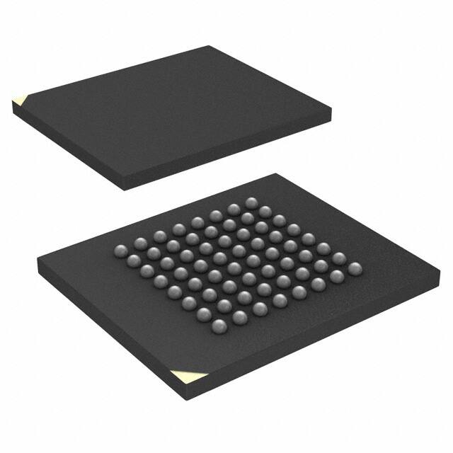
Figure 1: 64-Ball Easy BGA (8mm x 10mm x 1.2mm)
0.78 TYP
Seating
plane
0.1
1.00 TYP
64X Ø0.43 ±0.1
1.5 ±0.1
8
7
6
5
4
3
2
Ball A1 ID
Ball A1 ID
1
0.5 ±0.1
A
B
C
D
8 ±0.1
E
F
1.00 TYP
G
H
10 ±0.1
1.20 MAX
Note:
PDF: 09005aef8448483a
128_256_512_65nm_g18.pdf - Rev. E 8/11 EN
1. All dimensions are in millimeters.
13
Micron Technology, Inc. reserves the right to change products or specifications without notice.
© 2011 Micron Technology, Inc. All rights reserved.
�128Mb, 256Mb, 512Mb, 1Gb StrataFlash Memory
Signal Assignments
Signal Assignments
Figure 2: 64-Ball Easy BGA (Top View, Balls Down)
1
2
A1
A6
A2
3
4
5
6
7
8
A8
VPP
A13
VCC
A18
A22
VSS
A9
CE#
A14
A25
A19
A26
A3
A7
A10
A12
A15
WP#
A20
A21
A4
A5
A11
RST#
VCCQ
VCCQ
A16
A17
DQ8
DQ1
DQ9
DQ3
DQ4
CLK
DQ15
RFU
RFU
DQ0
DQ10 DQ11 DQ12 ADV# WAIT
OE#
A23
RFU
DQ2
VCCQ
DQ5
DQ6
DQ14 WE#
RFU
VSS
VCC
VSS
DQ13
VSS
DQ7
A
B
C
D
E
F
G
H
Notes:
PDF: 09005aef8448483a
128_256_512_65nm_g18.pdf - Rev. E 8/11 EN
1.
2.
3.
4.
5.
A24
A1 is the least significant address bit.
B6 is A25 for 512Mb densities and above; otherwise, it is a no connect (NC).
B8 is A26 for 1Gb density; otherwise, it is a no connect (NC).
G1 is A23 for 128Mb density and above; otherwise, it is a no connect (NC).
H8 is A24 for 256Mb density and above; otherwise, it is a no connect (NC).
14
Micron Technology, Inc. reserves the right to change products or specifications without notice.
© 2011 Micron Technology, Inc. All rights reserved.
�128Mb, 256Mb, 512Mb, 1Gb StrataFlash Memory
Signal Descriptions
Signal Descriptions
Table 4: Signal Descriptions
Symbol
Type
Description
A[MAX:1]
Input
Address inputs: Address inputs for all READ/WRITE cycles.
DQ[15:0]
Input/Output
Non-MUX
Data: Data or command inputs during WRITE cycles; data, status, or device information outputs during READ cycles.
A/D MUX
Address inputs: Upper address inputs for all READ/WRITE cycles.
A[MAX:16]
Input
ADQ[15:0]
Input/Output
Address or data: Lower address inputs during the address phase for all READ/WRITE
cycles; data or command inputs during WRITE cycles; data, status, or device information outputs during READ cycles.
CE#
Input
Chip enable: LOW true input. When LOW, CE# selects the die; when HIGH, CE# deselects the die and places it in standby.
OE#
Input
Output enable: LOW true input. Must be LOW for READs and HIGH for WRITEs.
WE#
Input
Write enable: LOW true input. Must be LOW for WRITEs and HIGH for READs.
CLK
Input
Clock: Synchronizes burst READ operations with the host controller.
ADV#
Input
Address valid: LOW true input. When LOW, ADV# enables address inputs. For synchronous burst READs, address inputs are latched on the rising edge.
WP#
Input
Write protect: LOW true input. When LOW, WP# enables block lock down; when
HIGH, WP# disables block lock down.
RST#
Input
Reset: LOW true input. When LOW, RST# inhibits all operations; must be HIGH for
normal operations.
VPP
Input
Erase/program voltage: Enables voltage for PROGRAM and ERASE operations. Array
contents cannot be altered when VPP is at or below VPPLK.
WAIT
Output
WAIT: Configurable HIGH or LOW true output. When asserted, WAIT indicates
DQ[15:0] is invalid; when de-asserted, WAIT indicates DQ[15:0] is valid.
VCC
Power
Core power: Supply voltage for core circuits. All operations are inhibited when VCC is
at or below VLKO.
VCCQ
Power
I/O power: Supply voltage for all I/O drivers. All operations are inhibited when VCCQ is
at or below VLKOQ.
VSS
Power
Logic ground: Core logic ground return. Connect all VSS balls to system ground; do
not float any VSS balls.
VSSQ
Power
I/O ground: I/O driver ground return. Connect all VSSQ balls to system ground; do not
float any VSSQ balls.
Control Signals
PDF: 09005aef8448483a
128_256_512_65nm_g18.pdf - Rev. E 8/11 EN
15
Micron Technology, Inc. reserves the right to change products or specifications without notice.
© 2011 Micron Technology, Inc. All rights reserved.
�128Mb, 256Mb, 512Mb, 1Gb StrataFlash Memory
Bus Interface
Bus Interface
The bus interface uses CMOS-compatible address, data, and bus control signals for all
bus WRITE and bus READ operations. The address signals are input only, the data signals are input/output (I/O), and the bus control signals are input only. The address inputs are used to specify the internal device location during bus READ and bus WRITE
operations. The data I/Os carry commands, data, or status to and from the device. The
control signals are used to select and deselect the device, indicate a bus READ or bus
WRITE operation, synchronize operations, and reset the device.
Do not float any inputs. All inputs must be driven or terminated for proper device operation. Some features may use additional signals. See Signal Descriptions for descriptions of these signals.
The following table shows the logic levels that must be applied to the bus control signal
inputs for the bus operations listed.
Table 5: Bus Control Signals
X = Don’t Care; High = VIH; Low = VIL
Bus Operations
RST#
CE#
CLK
ADV#
OE#
WE#
Address
Data I/O
Reset
Low
X
X
X
X
X
X
High-Z
Standby
High
High
X
X
X
X
X
High-Z
Output Disable
High
X
X
X
High
X
X
High-Z
Asynchronous Read
High
Low
X
Low
Low
High
Valid
Output
Synchronous Read
High
Low
Running
Toggle
Low
High
Valid
Output
Write
High
Low
X
X
High
Low
Valid
Input
Reset
RST# LOW places the device in reset, where device operations are disabled; inputs are
ignored, and outputs are placed in High-Z.
Any ongoing ERASE or PROGRAM operation will be aborted and data at that location
will be indeterminate.
RST# HIGH enables normal device operations. A minimum delay is required before the
device is able to perform a bus READ or bus WRITE operation. See AC specifications.
Standby
RST# HIGH and CE# HIGH place the device in standby, where all other inputs are ignored, outputs are placed in High-Z (independent of the level placed on OE#), and power
consumption is substantially reduced.
Any ongoing ERASE or PROGRAM operation continues in the background and the device draws active current until the operation has finished.
Output Disable
When OE# is deasserted with CE# asserted, the device outputs are disabled. Output pins
are placed in a high-impedance state. WAIT is deasserted in AD-muxed devices and
driven to High-Z in non-multiplexed devices.
PDF: 09005aef8448483a
128_256_512_65nm_g18.pdf - Rev. E 8/11 EN
16
Micron Technology, Inc. reserves the right to change products or specifications without notice.
© 2011 Micron Technology, Inc. All rights reserved.
�128Mb, 256Mb, 512Mb, 1Gb StrataFlash Memory
Bus Interface
Asynchronous Read
For RCR15 = 1 (default), CE# LOW and OE# LOW place the device in asynchronous bus
read mode:
•
•
•
•
RST# and WE# must be held HIGH; CLK must be tied either HIGH or LOW.
Address inputs must be held stable throughout the access, or latched with ADV#.
ADV# must be held LOW or can be toggled to latch the address.
Valid data is output on the data I/Os after tAVQV, tELQV, tVLQV, or tGLQV, whichever is
satisfied last.
Asynchronous READ operations are independent of the voltage level on V PP.
For asynchronous page reads, subsequent data words are output tAPA after the least significant address bit(s) are toggled: 16-word page buffer, A[3:0].
Synchronous Read
For RCR15 = 0, CE# LOW, OE# LOW, and ADV# LOW place the device in synchronous
bus read mode:
•
•
•
•
RST# and WE# must be held HIGH.
CLK must be running.
The first data word is output tCHQV after the latency count has been satisfied.
For array reads, the next address data is output tCHQV after valid CLK edges until the
burst length is satisfied.
• For nonarray reads, the same address data is output tCHQV after valid CLK edges until
the burst length is satisfied.
The address for synchronous read operations is latched on the ADV# rising edge or the
first rising CLK edge after ADV# low, whichever occurs first for devices that support up
to 108 MHz. For devices that support up to 133 MHz, the address is latched on the last
CLK edge when ADV# is low.
Burst Wrapping
Data stored within the memory array is arranged in rows or word lines. During synchronous burst reads, data words are sensed in groups from the array. The starting address
of a synchronous burst read determines which word within the wordgroup is output
first, and subsequent words are output in sequence until the burst length is satisfied.
The setting of the burst wrap bit (RCR3) determines whether synchronous burst reads
will wrap within the wordgroup or continue on to the next wordgroup.
PDF: 09005aef8448483a
128_256_512_65nm_g18.pdf - Rev. E 8/11 EN
17
Micron Technology, Inc. reserves the right to change products or specifications without notice.
© 2011 Micron Technology, Inc. All rights reserved.
�128Mb, 256Mb, 512Mb, 1Gb StrataFlash Memory
Bus Interface
Figure 3: Main Array Word Lines
16-Word sense group
16-bit data word
0x000030
0
1
2
3
4
5
6
7
8
9 A B
C
D
E
F
0x000020
0
1
2
3
4
5
6
7
8
9 A B
C
D
E
F
0x000010
0
1
2
3
4
5
6
7
8
9 A B
C
D
E
F
0x000000
0
1
2
3
4
5
6
7
8
9 A B
C
D
E
F
Word
lines
Address
Bit lines
256 bits
Figure 4: Wrap/No-Wrap Example
16-bit data word
2
3
4
5
6
7
8
9 A B
2
3
4
5
6
7
8
9 A B
Wrap
No wrap
End-of-Wordline Delay
Output delays may occur when the burst sequence crosses the first end-of-wordline
boundary onto the start of the next wordline.
No delays occur if the starting address is sense-group aligned or if the burst sequence
never crosses a wordline boundary. However, if the starting address is not sense-group
aligned, the worst-case end-of-wordline delay is one clock cycle less than the initial access latency count used. This delay occurs only once during the burst access. WAIT informs the system of this delay when it occurs.
Figure 5: End-of-Wordline Delay
0x000020
0
1
2
3
4
5
6
7
8
9 A B
C
D
E
F
0x000010
0
1
2
3
4
5
6
7
8
9 A B
C
D
E
F
EOWL delay
PDF: 09005aef8448483a
128_256_512_65nm_g18.pdf - Rev. E 8/11 EN
18
Micron Technology, Inc. reserves the right to change products or specifications without notice.
© 2011 Micron Technology, Inc. All rights reserved.
�128Mb, 256Mb, 512Mb, 1Gb StrataFlash Memory
Bus Interface
Write
CE# LOW and WE# LOW place the device in bus write mode, where RST# and OE# must
be HIGH, CLK and ADV# are ignored, input data and address are sampled on the rising
edge of WE# or CE#, whichever occurs first.
During a write operation in muxed devices, address is latched during the rising edge of
ADV# OR CE# whichever occurs first and Data is latched during the rising edge of WE#
OR CE# whichever occurs first.
Bus WRITE cycles are asynchronous only.
The following conditions apply when a bus WRITE cycle occurs immediately before, or
immediately after, a bus READ cycle:
• When transitioning from a bus READ cycle to a bus WRITE cycle, CE# or ADV# must
toggle after OE# goes HIGH.
• When in synchronous read mode (RCR15 = 0; burst clock running), bus WRITE cycle
timings tVHWL (ADV# HIGH to WE# LOW), tCHWL (CLK HIGH to WE# LOW), and
tWHCH (WE# HIGH to CLK HIGH) must be met.
• When transitioning from a bus WRITE cycle to a bus READ cycle, CE# or ADV# must
toggle after WE# goes HIGH.
PDF: 09005aef8448483a
128_256_512_65nm_g18.pdf - Rev. E 8/11 EN
19
Micron Technology, Inc. reserves the right to change products or specifications without notice.
© 2011 Micron Technology, Inc. All rights reserved.
�128Mb, 256Mb, 512Mb, 1Gb StrataFlash Memory
Command Definitions
Command Definitions
Commands are written to the device to control all operations. Some commands are
two-cycle commands that use a SETUP and a CONFIRM command; other commands
are single-cycle commands that use only a SETUP command followed by a data READ
cycle or data WRITE cycle. Valid commands and their associated command codes are
shown in the table below.
The device supports READ-While-WRITE and READ-While-ERASE operations with bus
cycle granularity, not command granularity. That is, both bus WRITE cycles of a two-cycle command do not need to occur as back-to-back bus WRITE cycles to the device;
READ cycles may occur between the two write WRITE cycles of a two-cycle command.
However, a WRITE operation must not occur between the two bus WRITE cycles of a
two-cycle command; this will cause a command sequence error (SR[7,5,4] = 1).
Due to the large buffer size of devices, the system interrupt latency may be impacted
during the buffer fill phase of a buffered programming operation. Please refer to the relevant Application Note to implement a software solution for your system
Figure 6: Two-Cycle Command Sequence
Address
Partition A
Partition A
Partition B
WE#
OE#
D/Q
Setup
Confirm
00FFh
Figure 7: Single-Cycle Command Sequence
Address
Partition A
Partition A
Partition B
WE#
OE#
D/Q
Setup
00FFh
Figure 8: READ Cycle Between WRITE Cycles
Address
Partition A
Partition B
Partition A
WE#
OE#
D/Q
PDF: 09005aef8448483a
128_256_512_65nm_g18.pdf - Rev. E 8/11 EN
Setup
Read data
20
Confirm
Micron Technology, Inc. reserves the right to change products or specifications without notice.
© 2011 Micron Technology, Inc. All rights reserved.
�128Mb, 256Mb, 512Mb, 1Gb StrataFlash Memory
Command Definitions
Figure 9: Illegal Command Sequence
Address
Partition A
Partition B
Partition A
Partition A
WE#
OE#
D/Q
Setup
Write data
Confirm
Status
Table 6: Command Set
Command
Code
(Setup/Confirm)
Description
Register Operations
PROGRAM READ CONFIGURATION REGISTER
0060h/0003h
Programs the read configuration register. The desired read configuration register value is placed on the address bus, and written to the read configuration register when the CONFIRM command is issued.
PROGRAM EXTENDED CONFIGURATION REGISTER
0060h/0004h
Programs the extended configuration register. The desired extended configuration register value is placed on the address bus,
and written to the read configuration register when the CONFIRM command is issued.
PROGRAM OTP AREA
00C0h
Programs OTP area and OTP lock registers. The desired register
data is written to the addressed register on the next WRITE cycle.
CLEAR STATUS REGISTER
0050h
Clears all error bits in the status register.
READ ARRAY
00FFh
Places the addressed partition in read array mode. Subsequent
reads outputs array data.
READ STATUS REGISTER
0070h
Places the addressed partition in read status mode. Subsequent
reads outputs status register data.
READ ID
0090h
Places the addressed partition in read ID mode. Subsequent
reads from specified address offsets output unique device information.
READ CFI
0098h
Places the addressed partition in read CFI mode. Subsequent
reads from specified address offsets output CFI data.
0041h
Programs a single word into the array. Data is written to the array on the next WRITE cycle. The addressed partition automatically switches to read status register mode.
00E9h/00D0h
Initiates and executes a BUFFERED PROGRAM operation. Additional bus READ/WRITE cycles are required between the and
confirm commands to properly perform this operation. The addressed partition automatically switches to read status register
mode.
Read Mode Operations
Array Programming Operations
SINGLE-WORD PROGRAM
BUFFERED PROGRAM
PDF: 09005aef8448483a
128_256_512_65nm_g18.pdf - Rev. E 8/11 EN
21
Micron Technology, Inc. reserves the right to change products or specifications without notice.
© 2011 Micron Technology, Inc. All rights reserved.
�128Mb, 256Mb, 512Mb, 1Gb StrataFlash Memory
Command Definitions
Table 6: Command Set (Continued)
Command
BUFFERED ENHANCED FACTORY
PROGRAM
Code
(Setup/Confirm)
Description
0080h/00D0h
Initiates and executes a BUFFERED ENHANCED FACTORY PROGRAM operation. Additional bus READ/WRITE cycles are required after the CONFIRM command to properly perform this
operation. The addressed partition automatically switches to
read status register mode.
0020h/00D0h
Erases a single, addressed block. The ERASE operation commences when the CONFIRM command is issued. The addressed partition automatically switches to read status register mode.
Lock Block
0060h/0001h
Sets the lock bit of the addressed block.
Unlock Block
0060h/00D0h
Clears the lock bit of the addressed block.
Lock-Down Block
0060h/002Fh
Sets the lock-down bit of the addressed block.
Block Erase Operations
BLOCK ERASE
Security Operations
Other Operations
SUSPEND
00B0h
Initiates a suspend of a PROGRAM or BLOCK ERASE operation
already in progress when issued to any device address
SR[6] = 1 indicates erase suspend
SR[2] = 1 indicates program suspend
RESUME
00D0h
Resumes a suspended PROGRAM or BLOCK ERASE operation
when issued to any device address. A program suspend nested
within an erase suspend is resumed first.
00BCh/00D0h
Performs a blank check of an addressed block. The addressed
partition automatically switches to read status register mode.
BLANK CHECK
PDF: 09005aef8448483a
128_256_512_65nm_g18.pdf - Rev. E 8/11 EN
22
Micron Technology, Inc. reserves the right to change products or specifications without notice.
© 2011 Micron Technology, Inc. All rights reserved.
�128Mb, 256Mb, 512Mb, 1Gb StrataFlash Memory
Status Register
Status Register
The status register is a 16-bit, read-only register that indicates device status, region status, and operating errors. Upon power-up or exit from reset, the status register defaults
to 0080h (device ready, no errors).
The status register has status bits and error bits. Status bits are set and cleared by the
device; error bits are only set by the device. Error bits are cleared using the CLEAR STATUS REGISTER command or by resetting the device.
To read from the status register, first issue the READ STATUS REGISTER command and
then read from the device. Note that some commands automatically switch from read
mode to read status register mode.
Table 7: Status Register Bit Definitions (Default Value = 0080h)
Bit
Name
15:10
Reserved
9:8
Partition program error
7
Device status
0 = Device is busy; SR[9,8,6:1] are invalid, SR[0] is valid
1 = Device is ready; SR[9:8], SR[6:1] are valid
6
Erase suspend
0 = Erase suspend not in effect
1 = Erase suspend in effect
5:4
Erase error/blank check
error
program error
(command sequence
error)
3
VPP error
2
Program suspend
1
Block lock error
0 = Block not locked during program or erase; operation successful
1 = Block locked during program or erase; operation aborted
0
Partition status
SR[7]/SR[0]
0 0 = Active PROGRAM or ERASE operation in addressed partition
BEFP: Program or verify complete, or ready for data
0 1 = Active PROGRAM or ERASE operation in other partition
BEFP: Program or Verify in progress
1 0 = No active PROGRAM or ERASE operation in any partition
BEFP: Operation complete
1 1 = Reserved
PDF: 09005aef8448483a
128_256_512_65nm_g18.pdf - Rev. E 8/11 EN
Description
Reserved for future use; these bits will always be set to zero
SR[9]/SR[8]
0 0 = Region program successful
1 0 = Region program error: Attempted write with object data to control
mode region
0 1= Region-program error: Attempted rewrite to object mode region
1 1 = Region-program error: Attempted write using illegal command
(SR[4] will also be set along with SR[8,9] for the above error conditions
SR[5]/SR[4]
0 0 = PROGRAM or ERASE operation successful
0 1 = Program error: operation aborted
1 0 = Erase error: Operation aborted; Blank check error: Operation failed
1 1 = Command sequence error: Command aborted
0 = VPP within acceptable limits during program or erase
1 = VPP < VPPLK during program or erase; operation aborted
0 = Program suspend not in effect
1 = Program suspend in effect
23
Micron Technology, Inc. reserves the right to change products or specifications without notice.
© 2011 Micron Technology, Inc. All rights reserved.
�128Mb, 256Mb, 512Mb, 1Gb StrataFlash Memory
Status Register
Clear Status Register
The status register has status bits and error bits. Status bits are set and cleared by the
device; error bits are only set by the device. Error bits are cleared using the CLEAR STATUS REGISTER command or by resetting the device.
Note: Care should be taken to avoid status register ambiguity. If a command sequence
error occurs while in erase suspend, SR[5:4] will be set, indicating a command sequence
error. When the ERASE operation is resumed (and finishes), any errors that may have
occurred during the ERASE operation will be masked by the command sequence error.
To avoid this situation, clear the status register prior to resuming any suspended ERASE
operation.
The CLEAR STATUS REGISTER command functions independent of the voltage level on
VPP. Issuing the CLEAR STATUS REGISTER command places the addressed partition in
read status register mode. Other partitions are not affected.
Table 8: CLEAR STATUS REGISTER Command Bus Cycles
Command
CLEAR STATUS
REGISTER
PDF: 09005aef8448483a
128_256_512_65nm_g18.pdf - Rev. E 8/11 EN
Setup WRITE Cycle
Address Bus
Setup WRITE Cycle
Data Bus
Device address
0050h
24
Confirm WRITE Cycle Confirm WRITE Cycle
Address Bus
Data Bus
–
–
Micron Technology, Inc. reserves the right to change products or specifications without notice.
© 2011 Micron Technology, Inc. All rights reserved.
�128Mb, 256Mb, 512Mb, 1Gb StrataFlash Memory
Read Configuration Register
Read Configuration Register
The read configuration register is a volatile, 16-bit read/write register used to select bus
read modes and to configure synchronous burst read behavior of the device.
The read configuration register is programmed using the PROGRAM READ CONFIGURATION REGISTER command. To read the read configuration register, issue the READ
ID command and then read from offset 0005h.
Upon power-up or exit from reset, the read configuration register defaults to asynchronous mode (RCR15 = 1; all other bits are ignored).
Table 9: Read Configuration Register Bit Definitions (Default Value = BFCFh)
Bit
Name
15
Read mode
14:11
Latency count
0 0 1 1 = Code 3
0 1 0 0 = Code 4
0 1 0 1 = Code 5
0 1 1 0 = Code 6
0 1 1 1 = Code 7 (default)
1 0 0 0 = Code 8
1 0 0 1 = Code 9
1 0 1 0 = Code 10
1 0 1 1 = Code 11
1 1 0 0 = Code 12
1 1 0 1 = Code 13
Other bit settings are reserved; see the table below for supported
clock frequencies
10
WAIT polarity
0 = WAIT signal is LOW-true (default)
1 = WAIT signal is HIGH-true
9
Reserved
8
WAIT delay
7:3
Reserved
2:0
Burst length
Description
0 = Synchronous burst mode
1 = Asynchronous mode (default)
Write 0 to reserved bits
0 = WAIT de-asserted with valid data
1 = WAIT de-asserted one clock cycle before valid data (default)
Write 0 to reserved bits
0 1 0 = 8-word burst, wrap only
0 1 1 = 16-word burst, wrap only
1 1 1 = Continuous-burst: linear, no-wrap only (default)
Other bit settings are reserved
Table 10: Supported Clock Frequencies
Latency Count Code
Clock Frequency
VCCQ = 1.7V to 2.0V
3
≤32.6 MHz
4
≤43.5 MHz
5
≤54.3 MHz
6
≤65.2 MHz
PDF: 09005aef8448483a
128_256_512_65nm_g18.pdf - Rev. E 8/11 EN
25
Micron Technology, Inc. reserves the right to change products or specifications without notice.
© 2011 Micron Technology, Inc. All rights reserved.
�128Mb, 256Mb, 512Mb, 1Gb StrataFlash Memory
Read Configuration Register
Table 10: Supported Clock Frequencies (Continued)
Latency Count Code
Clock Frequency
VCCQ = 1.7V to 2.0V
7
≤76.1 MHz
8
≤87.0 MHz
9
≤97.8 MHz
10
≤108.7 MHz
11
≤119.6 MHz
12
≤130.4 MHz
13
≤133.3 MHz
Programming the Read Configuration Register
The read configuration register is programmed by issuing the PROGRAM READ CONFIGURATION REGISTER command. The desired RCR[15:0] settings are placed on
A[15:0], while the PROGRAM READ CONFIGURATION REGISTER SETUP command is
placed on the data bus. Upon issuing the SETUP command, the read mode of the addressed partition is automatically changed to read status register mode.
Next, the CONFIRM command is placed on the data bus while the desired settings for
RCR[15:0] are again placed on A[16:1]. Upon issuing the CONFIRM command, the read
mode of the addressed partition is automatically switched to read array mode.
Because the desired read configuration register value is placed on the address bus, any
hardware-connection offsets between the host’s address outputs and the device’s address inputs must be taken into account. For example, if the host’s address outputs are
aligned to the device’s address inputs such that host address bit A1 is connected to address bit A0, the desired register value must be left-shifted by one (for example, 2532h